Introduction
The rapid increase in power density across artificial intelligence (AI) training and inference hardware has made direct liquid cooling (DLC) the standard thermal solution for high-density AI compute platforms. A single high-performance AI accelerator module now routinely dissipates several hundred watts to over 1,000 W under sustained workloads, and a fully populated AI compute rack can demand upward of 200 kW of cooling capacity. Recent articles in this magazine have examined chip-level bare-die jet cooling architectures for high-performance computation systems [1] and in-package direct-on-chip liquid cooling for AI accelerator chips [2]. Both treatments focus, appropriately, on the GPU (graphics processing unit) compute die as the primary thermal target. Yet every modern AI accelerator package includes a second class of thermally critical heat source that receives far less engineering attention: High Bandwidth Memory (HBM) stacks.
HBM achieves its extraordinary bandwidth by stacking multiple DRAM (dynamic random-access memory) dies vertically and connecting them through fine-pitch through-silicon vias (TSVs), co-packaged on a silicon interposer alongside the GPU die. This three-dimensional architecture creates a thermal challenge that is qualitatively different from that of the GPU die: heat generated deep inside the stack must conduct upward through multiple die interfaces before reaching an external cooling surface. The result is a persistent vertical temperature gradient that increased cold plate flow rate alone cannot eliminate. When HBM junction temperatures exceed safe limits (typically 85°C) the memory controller reduces bandwidth to prevent damage (GPU compute dies tolerate higher junction temperatures of 90–95°C, making HBM typically the binding thermal constraint). This directly degrades AI training throughput and diminishes the return on investment of an expensive compute cluster.
This article examines the thermal physics of HBM under DLC, the co-cooling challenges inherent to shared cold plate design, and practical design methods for thermal engineers working on current and next-generation AI accelerator platforms.
HBM Architecture and Its Thermal Implications
A modern HBM package consists of a base logic die at the bottom of the stack, with 8 to 16 active DRAM dies stacked above it using micro-bump or hybrid bond interconnects. The entire assembly is placed on a silicon interposer alongside the GPU die, with tens of thousands of micro-bump connections providing the high-speed memory interface. Figure 1 shows a cross-section schematic of this 2.5D packaging arrangement. Three thermal phenomena inherent to this architecture, distinguish HBM from conventional planar DRAM (in which a single DRAM die lies flat on a PCB with no vertical stacking).
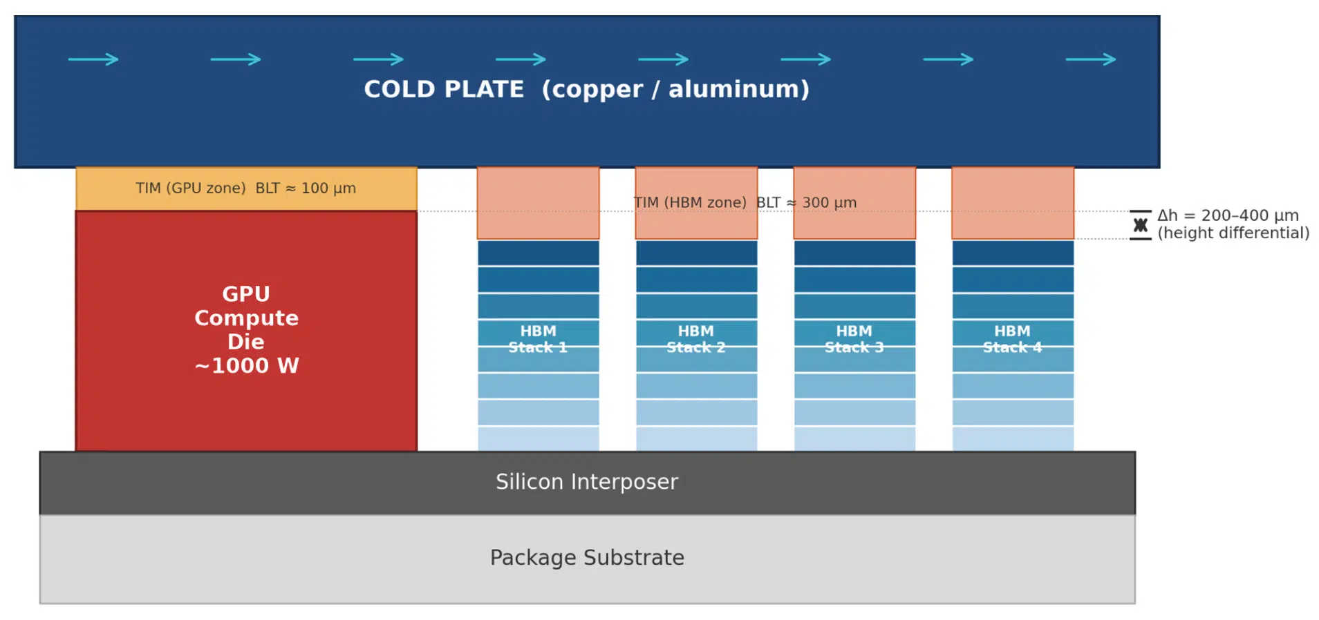
200–400 μm taller than the HBM stack top die, producing a thicker TIM layer and higher thermal resistance over the HBM zone.
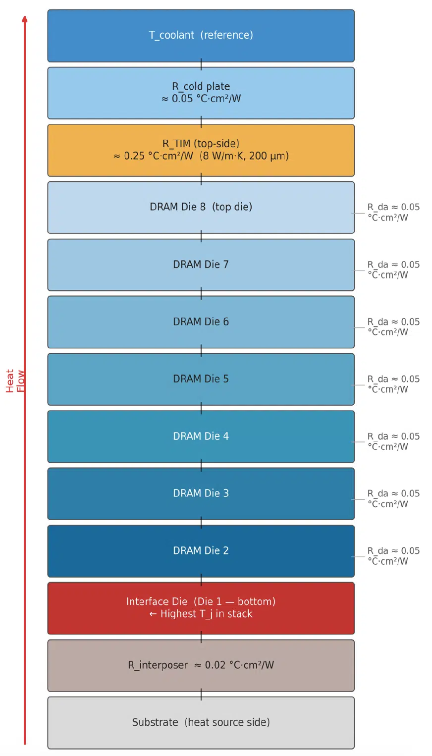
The first of these is vertical thermal resistance accumulation. Each DRAM die in the stack, typically 30 to 50 μm thick ,adds a layer of silicon, die-attach material, and underfill to the thermal path. In an 8-High (Hi) HBM stack – where “Hi” is the JEDEC-standard abbreviation for die layer count – heat generated at the interface die at the base must conduct upward through the full column before reaching the cold plate at the top. The cumulative junction-to-case thermal resistance of the stack can be three to five times higher than that of an equivalent planar die of the same footprint area. Figure 2 illustrates this additive resistance chain using a compact thermal resistor network model.
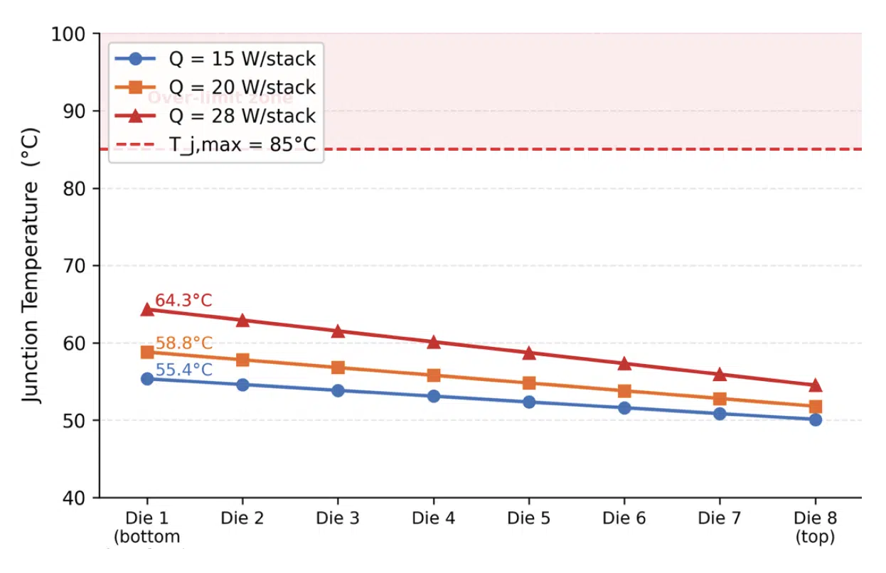
The second factor is the intra-stack temperature gradient. Because thermal resistance is additive through the stack, the bottom interface die consistently runs hotter than the top die under any workload. Figure 3 presents a representative temperature profile across die positions for an 8 Hi HBM stack at three dissipation levels with a 45°C coolant inlet. In HBM, power is dissipated across all active DRAM die layers rather than concentrated at the base; the bottom die runs hottest because its heat, and the heat from every layer above, must conduct upward through the above layers before reaching the cold plate. The bottom-to-top temperature differential ranges from 7°C to 14°C depending on stack height, die power distribution, and the quality of the top-side TIM and cold plate. This gradient means that a single junction temperature value is insufficient to characterize the stack thermally; the bottom-die temperature is always the binding thermal constraint.
The third significant factor is the lateral spreading limitation. The in-plane thermal conductivity of bulk silicon (approximately 150 W/m·K) and the thin die geometry constrain how effectively heat spreads within each DRAM die before propagating vertically. Workload-dependent memory access hot spots concentrate heat in a small die area and amplify the vertical gradient. A representative 8 Hi HBM stack dissipates approximately 15 to 30 W per stack under sustained bandwidth-intensive workloads. A typical AI accelerator module carries four to eight such stacks, placing the collective HBM thermal load at 60 to 240 W per module, a contribution that must be explicitly accounted for in any system thermal budget. Table 1 compares the key thermal parameters of the GPU die and HBM stack for a representative current-generation AI accelerator.
| Parameter | GPU Compute Die |
HBM Stack (per stack) |
|---|---|---|
| Typical power (W) | 700–1,000 | 15–30 |
| Footprint area (mm2) | 800–1,000 | 75–120 |
| Heat flux (W/cm2) | 80–120 | 15–25 |
| Max junction temp. (°C) | 95–105 | 85 |
| Height above interposer (µm) | 800–1,200 | 500–800 |
| Count per module | 1 | 4–8 |
| Primary thermal path | Top surface → cold plate |
Vertical stack (multi-die) |
| Key thermal challenge | High power density | Intra-stack gradient |
Table 1: Thermal comparison: GPU compute die vs. HBM stack (representative current-generation AI accelerator)
The Co-Cooling Challenge: One Cold Plate, Two Thermal Profiles
In the 2.5D packaging architecture used by current AI accelerators, both the GPU die and its surrounding HBM stacks share a single cold plate assembly. This creates a fundamental engineering tension: the GPU die and HBM stacks differ substantially in package height, heat flux, and maximum allowable junction temperature, as summarized in Table 1.
After assembly on the interposer, the GPU die typically stands 200 to 400 μm taller than the top die of the HBM stack. Height variation across HBM stacks in a manufacturing lot is substantially greater than for a monolithic GPU die. This is because each HBM stack undergoes 8 to 16 sequential die-bonding operations in which dimensional tolerances accumulate with each bond, TSV tip height varies due to wafer warpage during backside exposure, and individual DRAM dies — thinned to 30 to 50 μm — are susceptible to warpage that further alters post-bond height [3,4]. Without active compensation in the cold plate or TIM design, the cold plate contact force concentrates on the GPU die, leaving a thicker (and therefore higher-resistance) TIM layer over each HBM stack. For a compliant polymer TIM, with thermal conductivity of 8 W/m·K, a 200 μm increase in bond line thickness (BLT) over the HBM zone increases the TIM thermal resistance by approximately 2.5°C·cm²/W. This leads to a junction temperature penalty of 5°C at 20 W per stack, which represents a significant fraction of the total thermal margin between coolant temperature and the 85°C junction limit.
A second complication is differential thermal expansion under power cycling. The GPU die, HBM stacks, silicon interposer, and copper cold plate carry different coefficients of thermal expansion (CTE). As the package heats and cools during AI training runs, which alternate between high-power matrix operations and lower-power idle states, the assembly warps dynamically, altering the TIM contact geometry in ways that static assembly measurements cannot capture. Thermal qualification programs must therefore include repeated power cycling across the full operating temperature range to confirm that TIM pump-out and delamination do not progressively degrade performance over product lifetime.
Thermal Interface Material Selection for the HBM Zone
Thermal interface material selection for the HBM zone requires balancing thermal conductivity, mechanical compliance, and long-term reliability under repeated assembly cycles and power cycling. Table 2 compares five candidate materials across six operational parameters: conductivity, bond line thickness range, method of application, reworkability, cost, and handling requirements.
| Parameter | Conductivity (W/m·K) |
BLT Range | Method of Application |
Reworkability | Cost | Handling |
|---|---|---|---|---|---|---|
| Indium solder | 30–80 | 50–150 µm | Reflow or thermo-compression | Low – bond rework requires heating to >156°C | High | Soft metal; sensitive to voiding |
| CNT pad | 10–35 (⊥-plane) |
80–200 µm | Dry press-fit; no cure required | Good – peel and replace | High | Brittle; avoid shear stress during assembly |
| Polymer TIM (silicone/C-fiber) |
6–12 | 100–300 µm | Dispensed or pre-form; cured in-situ | Good – heat gun or solvent removal | Moderate | Standard PPE; no special precautions |
| PGS laminate | 8–10 (⊥-plane) |
50–150 µm | Adhesive bonded or pressed | Moderate – peelable if non-adhesive | Moderate–High | Brittle in bending; handle flat |
| Phase-change material (PCM) | 3–7 | 75–200 µm | Pre-form; melts at operating temp | Good – re-melts and reseats on reassembly | Low–Moderate | Store below phase-change temperature |
Table 2: TIM material comparison for the HBM zone in AI accelerator DLC packages (ordered by decreasing thermal conductivity)
Indium alloy solders (30 to 80 W/m·K) are applied by reflow or thermo-compression bonding, delivering the lowest contact resistance. Reworkability is limited, releasing a bond requires heating above 156°C, and cost is high; at the HBM zone, lower contact pressures raise voiding risk, making void inspection essential. Carbon nanotube (CNT) pads (10 to 35 W/m·K through-plane) require only dry press-fit application with no cure step; they are held by mechanical clamping load from the cold plate rather than adhesive; rework is peel-and-replace. CNT cost is also high and the fibrous pad must be handled without lateral shear to prevent delamination.
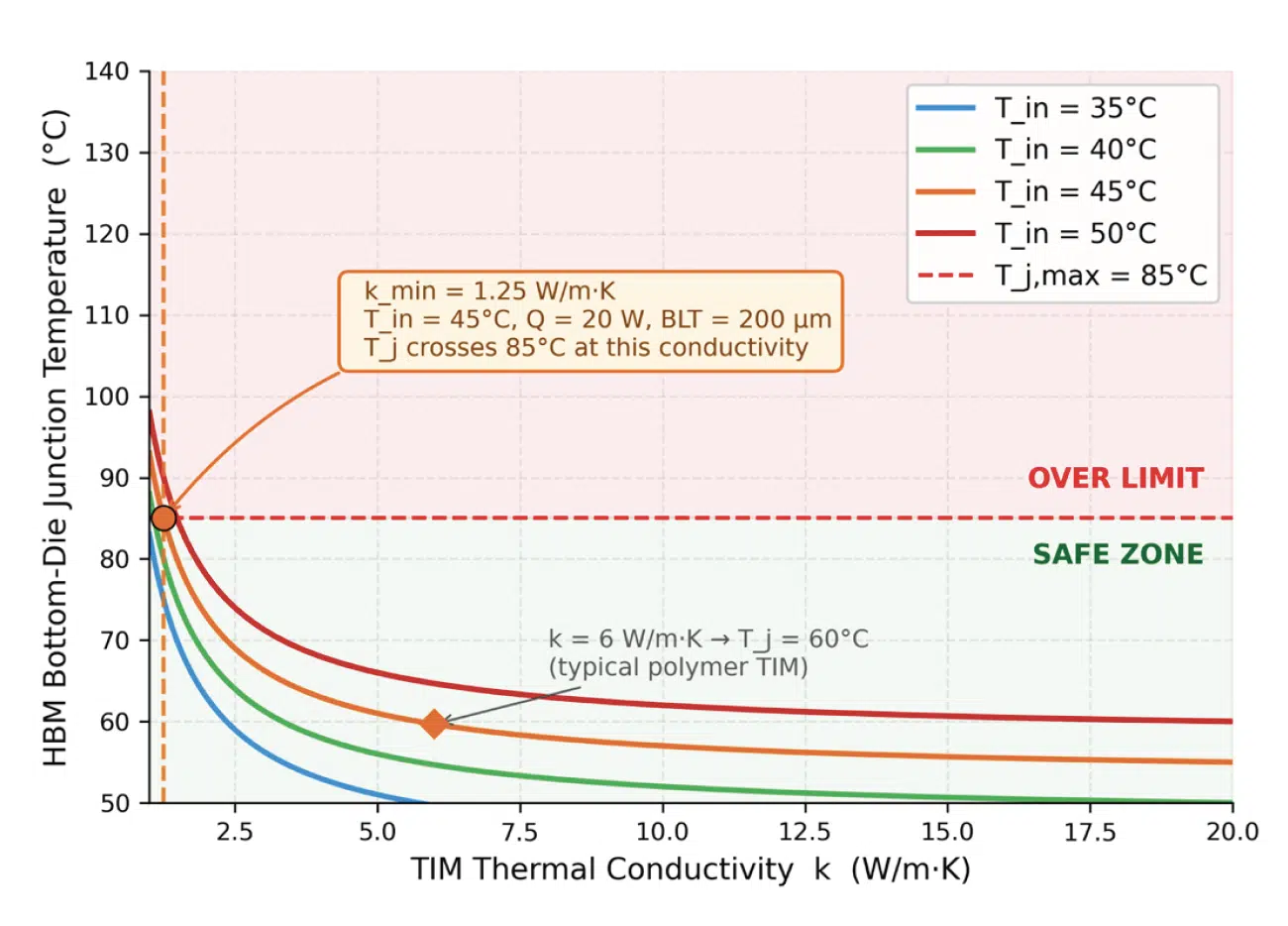
Polymer TIMs filled with carbon fiber or high-conductivity particles (6 to 12 W/m·K) are dispensed as a paste or supplied as a pre-form cured under assembly pressure. Reworkability is excellent, a heat gun or compatible solvent removes the material cleanly. Cost is moderate and handling requires only standard personal protective equipment. Figure 4 shows that at 45°C coolant inlet and 20 W per stack, the minimum effective bulk TIM conductivity (excluding contact resistance) to stay below the 85°C junction limit is 1.25 W/m·K, achievable across all material categories. Memory controllers typically begin pre-emptive bandwidth throttling at approximately 80°C, well before the 85°C hard limit, so even modest thermal margin beyond 1.25 W/m·K yields measurable performance benefit, but higher conductivity expands the margin for BLT variation and future power growth.
Pyrolytic graphite sheet (PGS) laminates (8 to 10 W/m·K through-plane; approximately 700 W/m·K in-plane) are adhesive-bonded or press-fit; their primary value is in the lateral spreading across the HBM footprint. Reworkability is moderate when non-adhesively-bonded, cost is moderate to high, and, because the laminate is brittle in bending, it must be handled flat. Phase-change materials (3 to 7 W/m·K) soften at operating temperature to conform to surface irregularities; reworkability is good since the material re-melts on disassembly, cost is low to moderate, and the only handling requirement is storage below the phase-change temperature. For all material types, the long term BLT stability needs to be verified through cross-sectional analysis conducted after 500 to 1,000 thermal cycles.
Cold Plate Flow Distribution
A DLC cold plate designed solely around the GPU die heat flux will systematically under-serve the HBM zones, and vice versa. Figure 5 illustrates the contrast between a single-zone flat-channel design and a bifurcated manifold architecture. The design philosophy follows directly from the guidance on server-level DLC flow budgeting in reference [1]: flow must be allocated in proportion to local heat flux, not package footprint area.
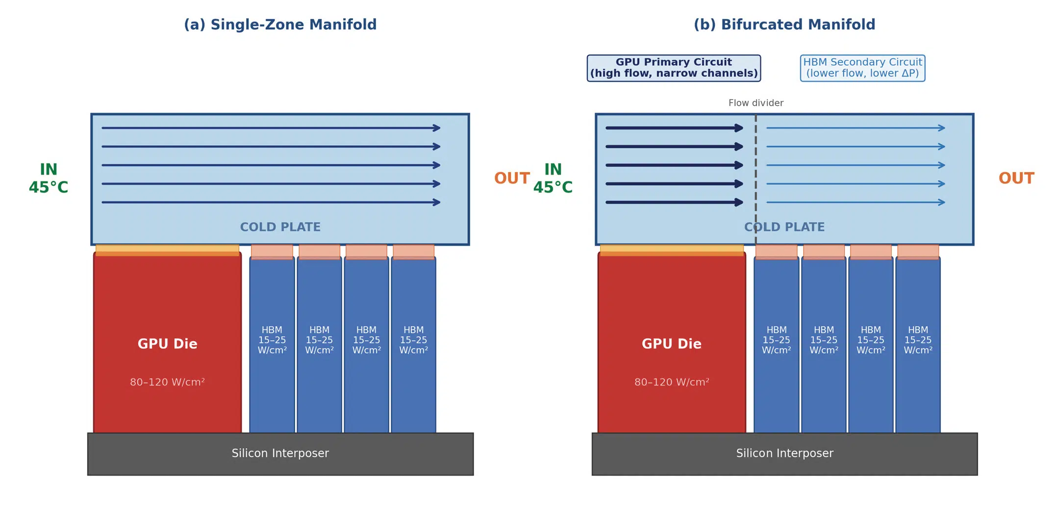
GPU and HBM zones. (b) A bifurcated design routes independently optimized flow to each zone, reducing total hydraulic pressure drop while
maintaining thermal margins at both the GPU and HBM zones.
The GPU die heat flux at full power can reach 80 to 120 W/ cm², requiring narrow, high-aspect-ratio channels (hydraulic diameter of 0.5 to 1.0 mm) with high mass flow rate to maintain junction temperatures within budget. The HBM stack heat flux, at approximately 15 to 25 W/cm² over a 75 to 120 mm² footprint per stack, is four to eight times lower. Routing the same high-velocity flow through the HBM zone wastes hydraulic pressure drop budget without providing proportionally more cooling. The recommended architecture is a bifurcated manifold that includes a primary high-flow circuit aligned with the GPU die footprint and a secondary lower-pressure-drop circuit covering the HBM zones.
Whether the secondary HBM circuit draws from the GPU zone outlet (series) or directly from the facility supply (parallel) depends on the thermal margin. When the flow is in series after the GPU, coolant arrives at the HBM zone 10 to 12°C warmer than 45°C facility inlet, leaving only about 18°C of margin to the 85°C HBM junction limit, which may be insufficient as HBM power budgets grow. In parallel, both circuits draw independently from the 45°C supply, preserving the full thermal margin for the HBM zone. Recall that the 7–14°C intra-stack temperature gradient (discussed in the HBM Architecture section) further erodes this margin: the 85°C limit applies to the bottom die, which already runs several degrees hotter than any coolant-side temperature reference. Figure 4 provides a direct method to determine which topology is needed: if a 10–12°C inlet rise would breach the 85°C limit at the operating TIM conductivity, parallel routing is required.
Thermal Modeling of HBM Stacks
Accurate thermal simulation of HBM under DLC requires explicitly resolving the intra-stack temperature gradient, a dimension that single-die CFD models collapse to a single node and therefore miss. Three modeling approaches are practical at different stages of the design process.
Compact resistor network models represent each die in the stack as thermal resistance nodes connecting the die power source to its upper and lower interfaces, as shown in Figure 2. These models run in seconds and are well-suited for system-level parametric sweeps to evaluate the sensitivity of bottom-die junction temperature to TIM conductivity, cold plate inlet temperature, stack height, and per-die power distribution. Figure 6 maps the design space as a function of TIM conductivity and stack height, with the 85°C junction limit overlaid as a contour.
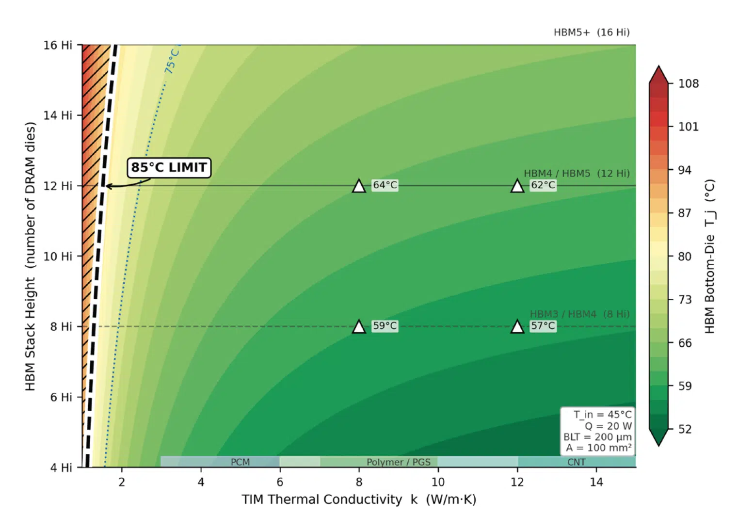
function of TIM conductivity (x-axis) and stack height expressed as number of die layers
(y-axis), computed from the compact resistor network model (T_in = 45°C, Q = 20 W/
stack, BLT = 200 μm, A = 100 mm²; resistance values from [3,7]). The dashed black
contour marks the 85°C junction limit. Horizontal lines indicate HBM4, HBM4E, and
HBM5 generation stack heights; vertical bands show the conductivity range of common
TIM material categories.
N-Source Compact Thermal Models for HBM
Industry practice for HBM thermal characterization follows the JEDEC DELPHI methodology (JESD15-4), which defines boundary-condition-independent compact thermal models (CTMs). Node count determines model resolution. A 2-source model (Rjc + Rjb) treats the whole stack as a single junction node, which is sufficient for package budgeting but unable to resolve intra-stack gradient (accuracy ~10–15% for junction temperature, Tj). A 3- or 4-source model adds a bottom-die node, enabling gradient prediction at ~5–8% accuracy. A 5-source model partitions the stack into distinct thermal zones (bottom die, lower DRAM group, upper DRAM group, top die, logic die interface), reaching ~4–6% accuracy and providing the resolution needed for memory-controller throttle calibration.
The N-source DELPHI CTM, which has one node per die layer, achieves the highest compact-model accuracy (within ~10% of full 3D simulation per JESD15-4 — comparable accuracy to a 2-source model for overall Tj, but with the per-die temperature resolution needed for throttle calibration) and is preferred for system co-simulation when die-level power maps are available [5,7]. Lasance (2008) reviews the construction methodology for multi-source packages [5].
Detailed finite element and computational fluid dynamics models resolve the individual die layers, TSV arrays, underfill, and cold plate flow field in three dimensions. These models are computationally expensive but necessary for predicting intra-die hot spots and for validating compact model accuracy at design corner conditions. Recent surrogate modeling techniques trained on full-resolution finite element datasets have demonstrated that intra-stack temperature gradients can be predicted within 2°C across a wide design space [6], making fast parametric optimization feasible without repeated high-fidelity simulations.
In-situ thermal monitoring completes the modeling workflow. Modern HBM generations include on-die temperature sensors that are accessible through the memory controller interface. These sensors provide a real-time proxy for bottom-die junction temperature and are invaluable for validating simulation predictions during system bring-up. Thermal validation platforms should log HBM die sensor readings alongside GPU die temperatures and CDU (coolant distribution unit) inlet and outlet coolant temperatures during sustained memory-bandwidth-intensive workloads, such as matrix-transpose microbenchmarks or streaming memory tests.
HBM Die Floor Planning for Thermal Management
The layout decisions made during HBM die floorplanning directly affect where heat is generated within each DRAM die, and therefore how severe the intra-stack gradient becomes in practice. Thermal considerations should inform floorplanning from the earliest design stage.
Memory bank arrangement relative to the TSV array is the most impactful floorplanning lever. TSVs act as high-conductivity vertical channels (copper at approximately 390 W/m·K versus silicon at 150 W/m·K), so concentrating high-bandwidth banks in the TSV-dense region reduces the lateral distance power dissipated from hot spots must travel before reaching a low-resistance vertical path [7]. Banks with correlated or simultaneous access patterns should be spatially interleaved, rather than grouped, to more uniformly distribute the power density across the die footprint and reduce peak local heat flux.
Power distribution network (PDN) routing affects thermal distribution indirectly: non-uniform resistive voltage drop (IR drop) creates a systematic power gradient that reinforces, rather than cancels, access-pattern hot spots. Co-optimizing PDN routing with bank placement to minimize IR drop variation is therefore both a signal-integrity and a thermal reliability practice.
Placing on-die temperature sensors adjacent to the highest-activity bank groups, rather than at a geometric center, ensures adaptive bandwidth throttling engages before the hottest location reaches the junction limit. At the perimeter, a thermal-relief keep-out zone free of high-power structures reduces edge-concentrated heat accumulation that is difficult to extract through the cold plate given the lower contact pressure at die edges [3].
Emerging Approaches for Future HBM Generations
As HBM evolves toward 12 to 16 Hi stacks and per-stack power budgets exceed 30 W with each successive generation, the industry is developing package-level solutions that address the intra-stack thermal resistance problem directly rather than relying solely on improvements to the external cold plate.
Integrated lateral thermal shunt elements (thermally conductive, electrically non-conductive inserts around high heat-concentration regions of the HBM package) provide a lateral bypass path that circumvents part of the vertical stack resistance. Implementations using silicon-based thermally conductive composites have demonstrated reductions in stack thermal resistance of 20 to 30% [8], directly extending thermal headroom at the same cold plate flow conditions.
Thermal through-silicon vias (tTSVs), electrically passive copper-filled vias distinct from signal-carrying TSVs, improve vertical thermal conductivity through the die column. Optimized tTSV density and placement have been shown to reduce junction-to-junction resistance by 23 to 47%, depending on fill fraction and layout [7]. Bottom-side heat extraction through embedded interposer cooling channels provides a direct thermal path from the bottom interface die, the hottest location, and has demonstrated bottom-die temperature reductions exceeding 20°C compared to top-only cooling under equivalent conditions [2].
Practical Guidelines
The following practices address HBM thermal performance across package design, workload characterization, controller configuration, and system-level cooling:
- Engage the package design team before die placement is finalized.
- Add a TIM retaining ring or raised interposer ledge around each HBM footprint to mechanically constrain cold plate lift-off and prevent progressive BLT growth under field thermal cycling.
- Specify on-die temperature sensor placement adjacent to high-activity bank groups rather than at a geometric center, so adaptive throttling triggers at the actual hottest location.
- Match interposer CTE to the cold plate material to minimize differential expansion at the TIM interface.
- Build HBM-specific thermal profiles for the AI workloads the platform will carry, logging HBM die sensor temperatures, GPU die temperatures, and memory bandwidth utilization during representative training and inference runs.
- Let the workload phase with the highest sustained HBM power – often large-batch matrix multiply with high memory reuse – drive the thermal design point rather than the datasheet thermal design power (TDP). These profiles reveal whether HBM or GPU die temperature is the binding constraint, directly determining the appropriate coolant routing topology.
- Configure the memory controller HBM throttling policy using measured die sensor data rather than default firmware settings.
- Set the primary throttle threshold at 80°C, 5°C below the 85°C hard limit, for proactive bandwidth reduction before T_j becomes a hard constraint.
- Build a derating curve mapping T_j to sustainable bandwidth fraction and expose it to the system power management layer, enabling real-time HBM bandwidth trade-offs during sustained high-density inference workloads without triggering hard shutdown.
- Size the coolant distribution unit explicitly for the HBM heat load; do not rely on GPU die thermal margins to absorb HBM power growth across generations.
- Specify 5-micron inline filters upstream of HBM cold plate microchannels to prevent particulate fouling that raises hydraulic resistance over time.
- For always-on AI inference clusters, provision a redundant pump circuit for the HBM cooling loop independent of the GPU die loop, so a single pump failure does not require full compute shutdown.
Conclusions
HBM stacks represent a growing and systematically underestimated contributor to the thermal budget of AI accelerator packages. As direct liquid cooling becomes universal in AI data centers and HBM stack heights continue to increase with each generation, treating HBM as an afterthought in cold plate design will increasingly result in memory bandwidth throttling during sustained AI workloads, which is precisely the condition where thermal management matters most.
The dominant physics of HBM heat transfer is vertical: heat generated at the bottom interface die must conduct upward through a column of stacked dies, accumulating resistance layer by layer, before it can be removed by the cold plate. No increase in external cold plate flow rate can fully overcome a high intra-stack resistance. The required interventions are at the package level: conformal cold plates, high-conductivity compliant TIMs, thermal TSVs, and lateral thermal shunt elements acting in combination. The bifurcated manifold design, N-source compact modeling methodology, TIM qualification approach, and die floorplanning practices described in this article provide a practical and extensible framework for thermal engineers tackling this challenge across current and next-generation AI accelerator platforms.
References
[1] Wei, T. “Design Considerations for Chip/Package Level Bare Die Impingement Cooling for High Performance Computation Systems.” Electronics Cooling, August 2024. https://www.electronics-cooling.com/2024/08/design-considerations-chip-package-level-bare-die-impingement-cooling-for-high-performance-computation-systems/
[2] “In-Package, Direct-on-chip Liquid Cooling with Lid-Compatible Manifold for Efficient AI Chip Thermal Management.” Electronics Cooling, Fall 2025.
[3] “Thermal Issues Related to Hybrid Bonding of 3D-Stacked High Bandwidth Memory: A Comprehensive Review.” Electronics (MDPI), Vol. 14, No. 13, 2682, 2025. https://doi.org/10.3390/electronics14132682
[4] Sekar, V. “Why is High Bandwidth Memory so Hard to Manufacture?” Vik’s Newsletter, Aug. 2025. https://www.viksnewsletter. com/p/why-is-hbm-so-hard-to-manufacture
[5] Lasance, C. J. M. “Ten Years of Boundary-Condition-Independent Compact Thermal Modeling of Electronic Parts: A Review.” Heat Transfer Engineering, Vol. 29, No. 2, pp. 149–168, 2008. (JEDEC JESD15-4 DELPHI methodology)
[6] “Neural Network Surrogate Model for Junction Temperature and Hotspot Position in 3D Multi-Layer High Bandwidth Memory Chiplets under Varying Thermal Conditions.” arXiv:2503.04049, March 2025.
[7] “On the Thermal Vulnerability of 3D-Stacked High-Bandwidth Memory Architectures.” arXiv:2509.00633, 2025.
[8] SK Hynix. “Integrated HBM Thermal Architecture: Integrated Cooling Elements for Reduced Package Thermal Resistance.” Technical Disclosure, May 2026.