As society is moving from fossil fuels to more sustainable electrical power, the systems for converting and delivering this electrical power are becoming increasingly important. These power electronic systems are responsible for controlling and shaping the electricity between the sources, such as solar and wind, and the end-use destination, such as driving a motor or charging the battery of your phone. The transistor is the fundamental building block of these converters. While silicon transistors thrive in computing applications, they have limitations when it comes to handling high power and high voltages. Many applications are very constrained in space and weight and the challenge is to get more power in a smaller package. Gallium nitride (GaN) transistors are key in achieving this goal, but its full potential remains untapped due to thermal limitations. The paradigm of cooling has long been about adding more material and going bigger: more metal, bigger heat sinks. Yet, the limitation on heat extraction often lies at the interfaces between these components. Instead, in this article we discuss the alternative path to improve cooling by not adding material, but by removing it. We evaluate several approaches of microchannel liquid cooling of GaN power devices and show the benefits of moving the cooling inside the chip.
Gallium nitride (GaN), a wide-band-gap semiconductor, has favorable material properties compared to silicon for power conversion. It enables faster-switching, smaller converters with lower losses. GaN technology, which originated from the Nobel-prize winning research on blue-light LEDs, has steadily matured over the last years. One such development is the capability to grow a thin, epitaxial layer of GaN on a low-cost silicon substrate, making the material cost effective in growth as well as in processing, since established silicon fabs can be utilized. This low-cost GaN-on-Si is the driving force behind the commercial adoption of GaN in power electronics.
Aside from the benefits of faster switching and lower losses, a unique property that distinguishes the GaN power transistor from its silicon counterpart is its lateral device structure. Transistors can be placed side-by-side on the same chip and assembled together into a power integrated circuit (Power IC), creating the potential of high-power converters integrated on a small chip. To fully appreciate this feature, we have to jump back to the early discovery of the transistor. Shortly after Shockley, Brattain and Bardeen demonstrated the first transistor, then-vice-president of Bell Labs, Jack Morton, spoke about the tyranny of numbers. For each extra component soldered together on a circuit, the system becomes more complex and likely to fail. The same factors hold for power converters: more complex topologies with multiple devices can improve efficiency, add functionality and reduce reliance on bulky passive components such as inductors. However, the higher component count is usually faced with reliability concerns. Just as the integrated circuit helped to manage the tyranny of numbers for processors, the GaN-based power IC may do the same for power conversion. One could imagine a centralized chip that contains all active high-voltage power switching components, potentially co-packaged with passive components such as capacitors [3]. A system like this could be a disruptive technology for power conversion, leading to more compact and powerful systems.
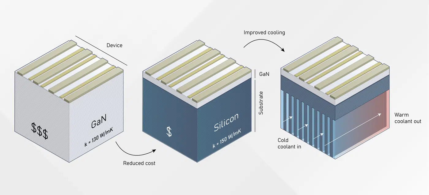
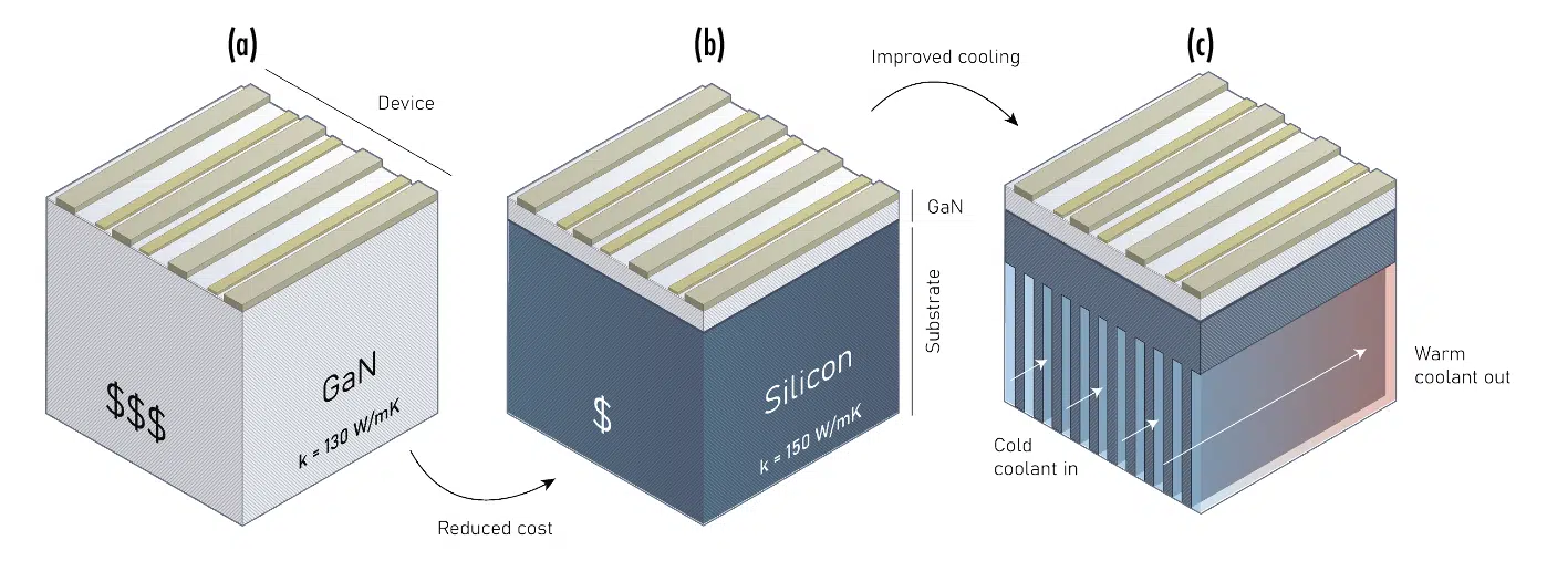
While this will be beneficial from a power density point of view, it aggravates the thermal challenges involved in maintaining junction temperatures at acceptable levels. Power dissipation will be concentrated in a single chip, so it cannot be spread to multiple large heat sinks. To fully exploit the possibilities of GaN-based power ICs, new strategies for effectively extracting the heat are required. Since GaN is grown as a thin layer on a silicon substrate, and this substrate has no functionality except for being an inexpensive carrier, it is possible to tap into the developments of in silicon microchannel heat sinks from past decades [1]. Microscopic cooling channels etched directly in the silicon substrate can function as a high-performance heat sink. The large surface-to-volume ratio of such microchannels provides high heat extraction while the absence of thermal interfaces ensures a low overall thermal resistance. In other words, it can turn the silicon substrate from a low-cost substrate into a high performance heat sink (Fig. 1).
Figure 1: (a) Bulk GaN, (b) GaN-on-Si reduces cost, (c) Embedded microchannels for improved cooling.
In this work we evaluate several embedded microchannel cooling approaches for GaN-on-Si power devices, and benchmark their performance. A useful non-dimensional metric for such benchmarking of cooling performance is the ratio of extracted power (Qmax = ΔTmaxRtotal)to pumping power (Ppump = fΔp) at a certain flow rate. This is known as the coefficient of performance (COP) and is given by the following formula:
COP = Qmax/PpumpRtotal = ΔTmax/fΔpRtotal
Rtotal is a summation of the individual contributions of thermal resistances between the power dissipating hot spot and the coolant at the system inlet. As the flow rate increases, Rtotal decreases, but Ppump quadratically increases due to dependency on both flow rate (f) and pressure drop (Δp). Ignoring any entrance effects, the COP can be seen as independent of die size. For example, two chips can be placed side-by-side, doubling both the maximum heat load and the flow rate, resulting in an equal COP. Plotting the COP against the maximum heat flux, qmax, provides a benchmark of heat extraction efficiency versus heat extraction capability.
qmax = Qmax/Adie
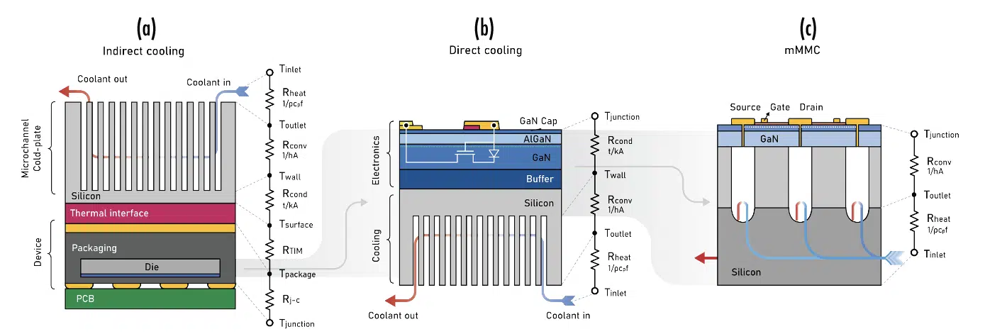
Figure 2 shows an overview of three approaches we compared using this approach. The first, in Fig. 2a shows an indirect cooling approach in which a silicon microchannel heat sink is attached with an intermediate thermal interface material (TIM) to a commercial packaged GaN transistor [4]. A one-dimensional thermal resistance network can be used to model the heat transfer between the device’s junction and coolant inlet. The junction-to-case thermal resistance (Rj-c) is given by the device manufacturer and consists of the various conductive elements between the hot-spot, die, and packaging layers.
Figure 2: (a) Indirect cooling, a microchannel cold plate is attached to a packaged die with an intermediate thermal interface material. (b) Direct die embedded microchannel cooling, cooling channels are etched inside the backside of the silicon substrate. (c) GaN-on-Si device with a monolithically integrated manifold microchannel inside the silicon substrate, co-designed with the electronics. Cooling channels are positioned below and aligned with the pads of the electronic device.
• RTIM describes the thermal resistance due to the TIM,
• Rcond accounts for the conduction in the silicon cold plate
• and Rconv accounts for the convective heat transfer between the solid silicon domain and the liquid coolant.
• Finally, Rheat is the thermal resistance due to the heat capacity of the coolant. Rheat scales with the flow-rate of the coolant (Rheat = 1/ρcpf) and does not depend on the geometry of the chip.
All the other thermal resistance components scale directly with the surface area of the chip, i.e., increasing chip size reduces these thermal resistances.
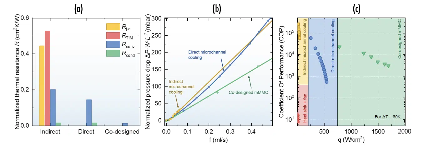
To compare multiple designs, we show the thermal resistance normalized by surface area in Fig. 3a. This shows that the major contributions in thermal resistance are related to the packaging and TIM, which account for more than 80% of the total. If the pressure drop of Fig. 3b is accounted for, this indirect method enables the extraction of about 55 W/cm2 at a COP value exceeding 104.
Figure 3: (a) Normalized thermal resistance components of indirect microchannel cooling, direct microchannel cooling and co-designed mMMC cooling. The components of R refer to the thermal resistance network diagrams illustrated in Fig. 1. (b) Normalized pressure drop (pressure drop multiplied by chip aspect ratio W/L) versus flow rate for the three configurations. (c) Benchmark of cooling efficiency (COP) versus maximum heat flux capability (q) for a maximum temperature rise of 60 K.
From this finding, it becomes clear that the most effective way to improve cooling is not by adding a better heatsink, but by removing the packaging and thermal interfaces. In the approach shown in Fig. 2b, similar 50 µm microchannels are directly embedded into the silicon substrate in the same approach initially proposed by Tuckerman [1]. The second column in Fig. 3a highlights the effectiveness of this approach: the contributions of Rj-c and RTIM are eliminated, resulting a substantial reduction in thermal resistance. Since similar channel dimensions are used as in the indirect approach, the pressure drop between the indirect and direct approach remain comparable (Fig. 3b). As a result, at a comparably high COP of 104, this direct approach achieves a 10-fold increase in maximum heat flux up to 500 W/cm2 (Fig. 3c) [5]. Furthermore, Fig. 3a reveals that the convective thermal resistance actually represents the limiting factor for heat extraction. We cannot scale the heatsink since the dimensions are constrained by the chip size. In order to reduce Rconv, smaller channel sizes can be utilized. However, this comes at a cost of increased pressure drop, which reduces COP and may add to system integration challenges.
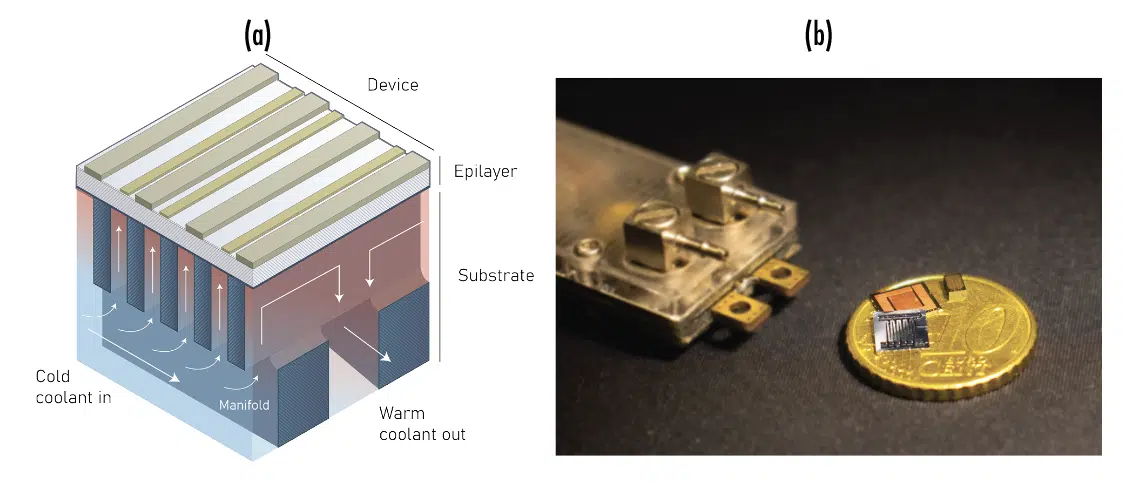
One potential approach to decouple Rconv and pressure drip is by utilizing a third dimension. The manifold microchannel heat sink (MMC) is a hierarchical design that addresses these issues. In a MMC, manifold channels distributes the liquid efficiently over the chip, reducing pressure drop and increasing temperature uniformity. However, design of such flow-hierarchy in MMC heat sinks traditionally require multiple bonded layers together. This is not only a cumbersome fabrication step, but also raises reliability concerns under repeated thermal cycling. In the third approach in Fig. 2c, we explored a new design approach, where the design of the cooling and electronics go hand-in-hand from the start of the fabrication. We monolithically integrated an MMC structure in a GaN-on-Si device, which we call mMMC, using a new fabrication method that exploits the etching selectivity between silicon and GaN [6]. The typical source-drain spacing of GaN transistors and the optimal range of microchannel pith are both in the range of 15 to 25 microns. We exploited this fact by etching small trenches through the GaN epilayer, realizing a cooling channel in the underlying silicon substrate, and finally sealing the trenches in the GaN epilayer during the metallization step. Using this approach, each source and drain of the transistor is linked to an individual cooling channel (Fig. 4a). We refer to this approach as a microfluidic-electronic co-design. The bonding interface between the manifold and the microchannels was eliminated and the entire 3D cooling structure was realized in a single silicon crystal. This monolithic structure ensures structural integrity as well as excellent heat transfer. Fig. 3a shows the substantial reduction in Rconv realized using this approach, as well as the reduction in pressure drop (Fig. 3b). Combining these properties, we can show an additional increase in maximum heat flux of almost 3-fold at a COP of 104, relative to the microchannels etched in the back of the substrate.
Figure 4: GaN power device with microfluidically co-designed mMMC. (a) Schematic of the mMMC structure. (b) Picture of a fabricated GaN power device with mMMC cooling.
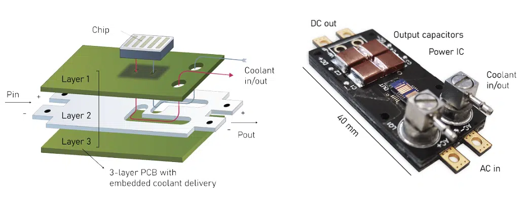
GaN has the potential to reshape power electronic, and improved cooling can be an enabling technology that facilitates this technology. The silicon substrate on which GaN is grown does not need to merely be an economic choice; in addition, it can become an efficient heat sink that pushes the boundaries of what is possible in terms of integration and power density. As an example, Fig. 5 shows an integrated GaN-based power rectifier with embedded microchannel cooling. Here, the GaN chip contains multiple power diodes, which are all cooled with water flowing inside the chip. Several challenges need to be addressed in terms of packaging and reliability in order to see such technology materialize, but at least it’s sure that cooling doesn’t need to be the limiting factor in a future with more compact and efficient power conversion.
Figure 5: 1.2 kV/120 W GaN-based full-wave bridge rectifier (FWBR) power IC with embedded microchannel cooling. Schematic (left) and prototype (right)
References:
[1] D. B. Tuckerman and R. F. W. Pease, “High-performance heat sinking for VLSI,” IEEE Electron Device Lett., vol. 2, no. 5, pp. 126–129, May 1981.
[2] D. B. Tuckerman et al., “Microchannel Heat Transfer: Early History, Commercial Applications, and Emerging Opportunities,” in ASME 2011 9th International Conference on Nanochannels, Microchannels, and Minichannels, Volume 2, 2011, pp. 739–756.
[3] R. Reiner and B. Weiss, “PCB-Embedding for GaN-on-Si Power Devices and ICs,” CIPS 2018; 10th Int. Conf. Integr. Power Electron. Syst., p. 6, 2018.
[4] R. Van Erp, G. Kampitsis, and E. Matioli, “Efficient Microchannel Cooling of Multiple Power Devices with Compact Flow Distribution for High Power-Density Converters,” IEEE Trans. Power Electron., vol. 35, no. 7, pp. 7235–7245, 2020.
[5] R. Van Erp, G. Kampitsis, L. Nela, R. S. Ardebili, and E. Matioli, “Embedded Microchannel Cooling for High Power-Density GaN-on-Si Power Integrated Circuits,” in InterSociety Conference on Thermal and Thermomechanical Phenomena in Electronic Systems, ITHERM, 2020, vol. 2020-July, pp. 53–59.
[6] R. van Erp, R. Soleimanzadeh, L. Nela, G. Kampitsis, and E. Matioli, “Co-designing Electronics with Microfluidics for More Sustainable Cooling,” Nature, vol. 586, no. 7824, 2020.
