Steady state operating temperature is a critical design parameter for ensuring the reliable operation of modern electronics systems. However, in practice it is but one of many factors that impact overall system health and performance. Modern challenges, like the large transient power draw associated with artificial intelligence (AI) workloads create the potential for more discontinuous failures that occur when these spikes damage sensitive components [1]. Likewise, the temperature-dependent warpage of modern highperformance compute and AI chip architectures cause stochastic voiding and nonuniformity in thermal interface material (TIM) bond line thickness that degrades efficiency and reliable operation [2]. These new paradigms create an urgent need to rethink thermal design priorities and consider new solutions that enable the industry to achieve performance and cost goals.
As a starting point, it is important to understand that electronics systems are designed to optimize performance rather than temperature. Performance, writ large, is a function of the available power in a system. While it is certainly not true that more power directly yields more performance, it generally holds that with all other variables constant, increasing system performance requires more power consumption. In any electronics component of a fixed design, one can select a parameter related to system performance, for example voltage, frequency (clock rate), utilization, or current (in power electronics) and find that increasing this parameter will also increase power consumption. Temperature is inextricably coupled to this available power as the consumed power must be dissipated from the system as heat. As a final corollary, the steady state operating temperature of a system is a combination of the cooling solution effectiveness and the system power consumption.
To manage this temperature rise, for a given power consumption, one can engineer thermal solutions of varying types to drive system operating temperatures higher or lower, but this does not in itself change the capability or performance of the system.
How then does one decide which temperature to design towards in designing a cooling solution? For decades, peak allowable temperatures for various systems and sectors (e.g. high-performance, consumer, mobile, etc.) were agreed upon through consensus-based engineering, for example via industry road mapping efforts [3-6]. Typically, this is an effort in balance, looking at specific failure modes of the affected hardware, expected system power and power densities, available and deployed cooling technologies, and presumed reliability targets for the sectors where the technology is deployed. These considerations are then distilled into a maximum allowable junction temperature for various technologies and sectors.
The Link Between the Arrhenius Relationship and Semiconductor Reliability; Origins and Relevance Today
It is commonly accepted that when it comes to device operating temperature, lower is better, across the board. This thinking arises from the often implicit assumption that an Arrhenius relationship exists between failure rates and temperature [6,7]. The Arrhenius equation suggests that the rate of certain temperature dependent processes, e.g. failure mechanisms in electronics, follows an exponential relationship with temperature:
Here, Ea represents the activation energy of the failure mechanism, k is Boltzmann’s constant, and T is the absolute temperature. This model underpins the widely cited “10°C rule,” which states that failure rates double for every 10°C increase in temperature.
A number of limitations for employing this model exist and will be examined in this review, but the most significant may be that this relationship can only be considered for a single failure mode at a time. At the system level, numerous failure modes will always co-exist, some of which do not follow this Arrhenius relationship. As such, simply lowering temperatures by a few degrees does not commonly result in increased lifetimes.
In the opposing direction, there is often the perception that if additional thermal margin exists, it will and should be consumed by increasing the power consumption of the target component (e.g. over clocking, over driving etc.). This ignores the reality that product lifetimes are typically set at a system level, and operating outside of a rigorously tested design window is prone to reduced stability and reliability of the system, netting a reduction in overall productivity over time.
Even within the subset of failure modes that do follow an Arrhenius relationship, the activation energy for these failures is not constant [8]. Along with this wide range of activation energies, most also have more than one accelerating factor. As such, predicting an improvement in system lifetimes based on arbitrarily lowering temperature rarely results tangible gains. The most practical use of this Arrhenius relationship is in the design of accelerated lifetime tests to determine mean time to failure (MTTF) for new designs undergoing reliability qualification and testing. The JEDEC standard JESD88E formalizes the calculation of an acceleration factor (AF), which is used to estimate how long it takes for a failure to occur in a high-stress test environment compared to the time it would take under normal field conditions at a lower temperature [9]:
Now considering the typical operating temperature of electronics of around 100°C and an activation energy of approximately 1, an acceleration factor of approximately 2 arises from Equation 2 [9]. Hence the oft-repeated heuristic that a 10°C reduction in temperature will double device lifetime. This heuristic, however convenient and grounded in apparently sound logic it may appear, often results in an overly simplistic and ultimately inaccurate analysis.
None of this is to suggest that the temperature limits that have been selected for semiconductors are invalid. As noted above, years of research, collaboration, and testing have gone into selecting and validating these parameters such that electronics systems will consistently deliver relevant operating lifetimes. What specifically needs to be examined more carefully is the notion that continually lowering temperatures will truly deliver more reliable systems, and if this focus on lower steady state temperatures should indeed be the focus of thermal system design.
Enjoying this article?
Subscribe to Electronics Cooling for practical, engineer-focused insight on today’s thermal management challenges—plus immediate access to new digital magazine issues.
Subscribe here →
Beyond Arrhenius: Real-World Considerations for Optimizing Reliable Performance
In the next section, we will consider failure mechanisms that do not follow the Arrhenius relationship. This serves to answer the driving question: “if we accept that the steady state peak operating temperatures that have been rigorously defined over the last 3 decades of industry road mapping are aligned with systems that can and will operate reliably, what other considerations are most important to consider for effective thermal design today?”
Non-Arrhenius Failure Mechanisms
A substantial fraction of electronic failures involve mechanisms that deviate from Arrhenius kinetics. We will investigate three of the most important mechanisms, namely:
- Thermomechanical fatigue
- Thermal gradients
- Hotspots
Thermal Cycling: The Fatigue Multiplier
Repeated thermal cycling induces stress at material interfaces due to mismatches in coefficients of thermal expansion (CTE). For example, solder joints exposed to power cycles that drove an 80°C temperature swing (all while remaining under the steady state operating temperature limits) resulted in reductions in MTTF of up to 3.7x when a suboptimal solder material was selected for die or substrate attach in a SiC IGBT [10]. Notably, these failures were not only direct functional failures (e.g. increase in device resistance due to cracking), but commonly increased device thermal resistance such that it could no longer operate within its design temperature limits at rated operating conditions.
This distinction is important. Focusing a design simply on time zero temperature, i.e., device operating temperature when a system is new, neglects to consider that if sufficient attention is not given to the lifetime performance of the thermal solution, those safe operating limits may be quickly exceeded. This concern is especially relevant at interfaces, where cyclic fatigue is constantly challenging a component’s ability to communicate with the thermal solution. Of note, modern AI chip architectures exhibit warpage that changes significantly as a function of temperature, which only exacerbates problems associated with cyclic fatigue.
Cycling-induced failures correlate strongly with the Coffin-Manson relationship:
Where Nf is cycles to failure, Δϵp is plastic strain range, and C and n are material constants. Plastic strain is not only a challenge for solders. Commonly, thermal interface materials (TIMs) such as phase change materials (PCMs) undergo plastic strain when subjected to cyclic stress due to temperature cycling and temperature dependent properties of the materials (e.g., viscosity). This can result in pumping of the TIM out of the interface (pump out) or separation of conductive fillers from the surrounding polymer matrix (dry out). Both mechanisms result in voids and loss of performance over time, increasing device operating temperature, sometimes seeing local increases of up to 3x [11].
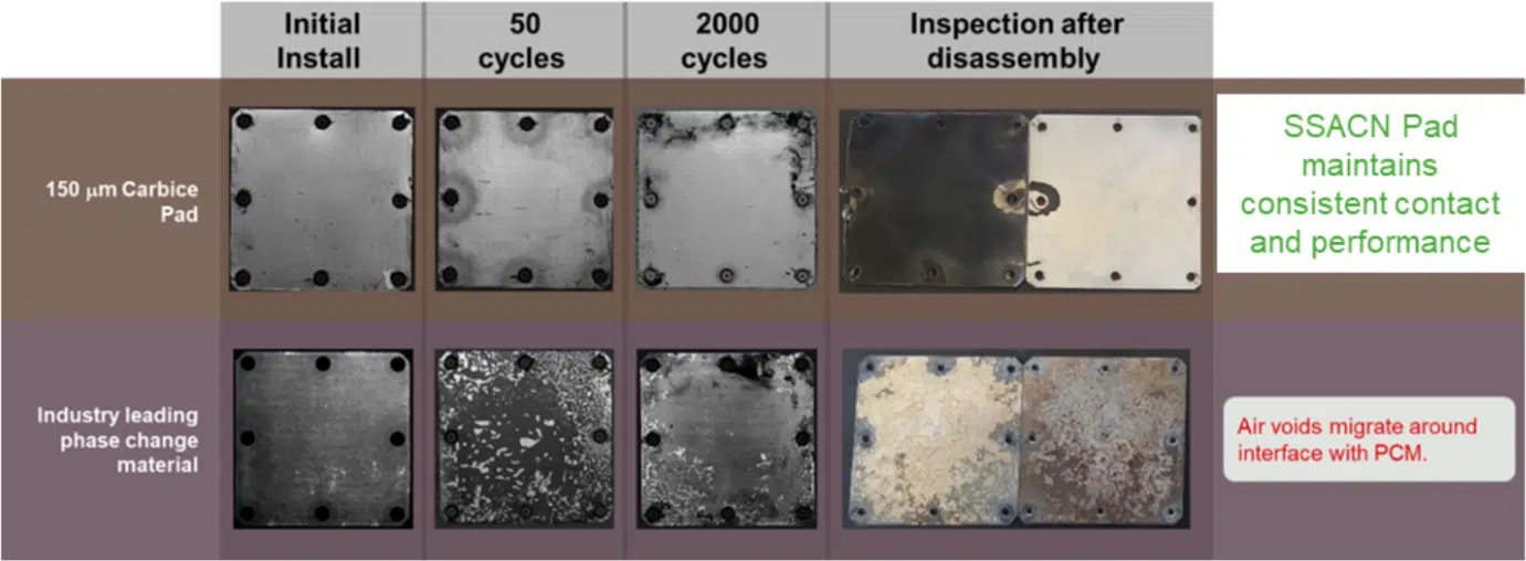
It is important then to utilize elastic TIMs that are not subject to this plastic deformation mechanism when seeking to maximize lifetime system performance. Substrate supported aligned carbon nanotubes (SSACN) meet this important requirement. Revisiting the Coffin-Manson relationship above, we see that when operated within their elastic range, i.e., driving Δϵp to zero, the number of cycles to failure goes towards infinity, effectively eliminating this failure mode.
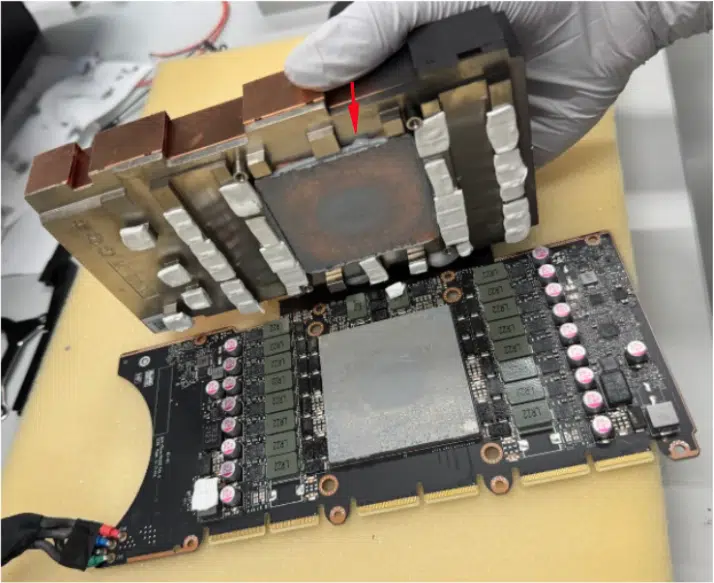
To demonstrate this characteristic, an accelerated life test was conducted where a 150 μm SSACN thermal pad from Carbice and an industry leading PCM were bolted between two plates with dissimilar CTE (Al and Invar). A description of the test setup and methodology can be found at [12]. The bolted joint was cycled 2000 times from -55°C to 110°C, with periodic in situ inspection of the interface coverage through acoustic microscopy. While both specimens had uniform coverage at the beginning of the test, the PCM rapidly developed voids that migrated around the interface throughout the duration of the test. These voids map to areas of localized loss of contact in the interface where hotspots and failures may occur in functional systems. The SSACN, on the other hand, maintained consistent coverage throughout the test (Figure 1a). Similar PCM nonuniformity can be found on contemporary GPUs (Figure 1b).
Thermal Gradients: The Silent Accelerant
Thermal gradients are a driving factor for both diffusion-driven and stress-related failures in electronics systems. For example, a thermal gradient of 0.29ºC/μm across a C4 interconnect reduces MTTF by an order of magnitude, as compared to a solder bump at a slightly higher temperature but lower thermal gradient of 0.11ºC/μm, due to enhanced atomic diffusion along the temperature gradient [13]. Similar thermal migration concerns exist within the semiconductor package in, for example, copper interconnects. As a comparison to steady state temperature, one model suggests that a gradient of 0.09ºC/μm in an interconnect is equivalent to an increase in temperature of 6°C in the absence of thermal gradients [14].
Given this stark contrast, it is imperative that effective thermal solutions deliver temperature uniformity, along with maintaining temperatures within limits. Certainly, this starts with avoiding the presence and generation of voids, as discussed above. However, lateral heat spreading is yet another powerful design tool that should be employed to homogenize temperatures across the die. Figure 2 shows a comparison of temperature distributions using an SSACN and a common PCM in a curved thermal test vehicle with a footprint comparable to a modern AI GPU. Heat spreading in the SSACN allows greater uniformity in the device while maintaining similar peak temperatures. TIMs with high in-plane thermal conductivity that spread heat over a broader area, resulting in lower in-package thermal gradients, will pay dividends in system lifetime performance. The aluminum core in the SSACN Pad delivers metal-like 200 W/mK heat spreading capability without the plastic deformation and creep failure modes from which metal TIMs can suffer.
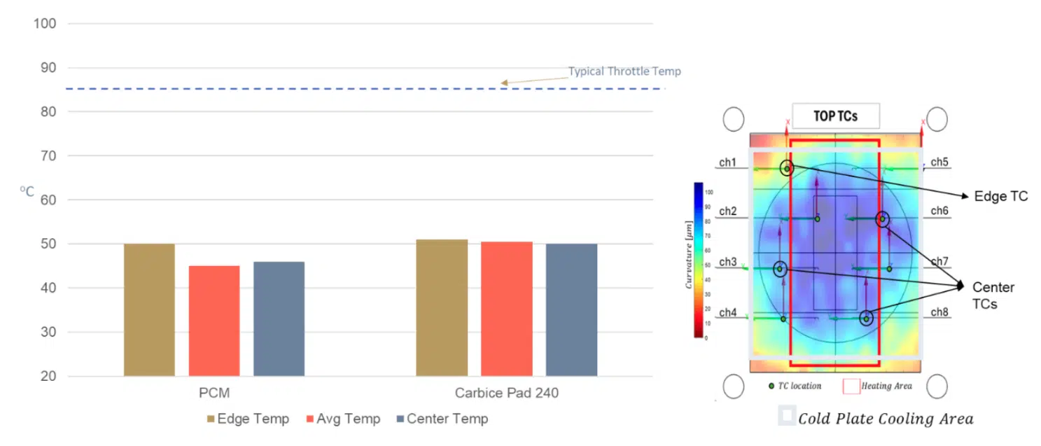
mm thermal test vehicle with 110 μm curvature (to simulate “hot curvature”) coupled to
a liquid cooled cold plate using a PCM TIM vs SSACN with heat spreading capability. 22
W/cm2 power density; 40°C inlet temperature
Localized Hotspots
Transistor-level power densities and grouping of functional devices within the die create micron-scale hotspots that are up to 10x the average power density of the die [15]. Traditional design thinking often results in strategies that simply bring temperatures as low as possible with a uniform approach to cooling the chip. However, employing such a strategy with such a highly nonuniform power map generally causes overcooling the areas of low power density. This exacerbates the thermal gradients that we seek to avoid, as well as wasting cooling resources (i.e. power, hardware, fluid capacity, etc.). Here again, TIMs that can effectively spread heat are an attractive solution. Secondarily, employing solutions that can strategically target areas of high or low power density, or high vs low warpage, with interface solutions matched to the local requirements delivers a solution that better that meets package requirements rather than coarsely targeting temperature minimization that ignores system performance and reliability needs.
Comparative Analysis of Failure Drivers
| Parameter | Impact on MTTF | Dominant Failure Modes | Arrhenius Compatibility |
|---|---|---|---|
| Bulk Temperature | 1.2x reduction per 10°C rise above maximum allowable temperature [9] | Electromigration, corrosion | High |
| Cycling (ΔT ~ 100°C) | 2–4x reduction [10,16] | TIM pump out or dry out, solder joint fatigue, via cracking | None |
| Thermal Gradients (0.3°C/μm) and Hotspots | 3–10x acceleration [13,14,17] | Interfacial delamination, cracking, gate oxide breakdown, hot carrier injection | Low |
Conclusion
While the Arrhenius equation remains a valuable tool for modeling temperature-activated chemical degradation processes, it does not address factors such as mechanical stresses, localized heating, and transient thermal profiles that can cause failures in modern electronics. Parameters such as hotspots (localized energy concentration), thermal gradients (spatial energy distribution), and thermomechanical cycling or rapid shock (temporal energy fluctuations) have emerged as dominant factors in contemporary failure analyses. Accordingly, engineers need to adopt a holistic, multi-physics approach to thermal design that integrates thermal, mechanical, and materials science principles to maximize device reliability and accurately predict and mitigate electronic failures in advanced systems. Part of this design approach should include incorporating hardware specifically engineered to address the most critical and relevant stressors associated with failure, i.e. thermal cycling and shock induced stress, lateral thermal gradients, and localized hot spotting in the case of high-power density chips. Of note, the combination of extremely high lateral conductivity, conformal compressibility, and cohesive integrity make aligned carbon nanotube arrays on metal foil uniquely suited to addressing these thermal challenges and distinguish it from other thermal interface materials as an optimum solution for device reliability and longevity.
References
[1] Li, Yuzhuo, and Yunwei Li. “AI Load Dynamics–A Power Electronics Perspective.” arXiv preprint arXiv:2502.01647 (2025).
[2] Islam, Nokibul, Choong Kooi Chee, and JoonYoung Choi. “Advanced Thermal Management for High Power HPC, AI.” 2025 IEEE 75th Electronic Components and Technology Conference (ECTC). IEEE, 2025.
[3] Hoefflinger, B. (2011). ITRS: The International Technology Roadmap for Semiconductors. In: Hoefflinger, B. (eds) Chips 2020. The Frontiers Collection. Springer, Berlin, Heidelberg. https://doi.org/10.1007/978-3-642-23096-7_7
[4] Wesling, Paul. “The Heterogeneous integration roadmap: Enabling technology for systems of the future.” 2020 Pan Pacific Microelectronics Symposium (Pan Pacific). IEEE, 2020.
[5] Malik, Azmat. “iNEMI Roadmap Identifies Trends Impacting Electronics Thermal Management.” Now You Can Cool Your Electronic Devices at the Component Level (2016).
[6] Pershing, A. V., and G. E. Hollingsworth. “Derivation of Delbruck’s Model for Random Failure (For Semiconductor Materials): Its Identification with the Arrhenius Model; and Its Experimental Verification.” Second Annual Symposium on the Physics of Failure in Electronics. IEEE, 1963.
[7] Toye, Charles R. Computerized Arrhenius Reliability Extrapolation Techniques. Vol. 4902. National Aeronautics and Space Administration, 1968.
[8] Activation energy defined; activation energies of failure mechanisms. https://www.eesemi.com/activation-energy.htm
[9] Wilcoxon, R. (2017, October 20). Does a 10°C increase in temperature really reduce the life of electronics by half? Electronics Cooling. https://www.electronics-cooling.com/2017/08/10c-increase-temperature-really-reduce-life-electronics-half/
[10] L. E. Kegley et al., “Comparison of Silicon Carbide Packages with Different Solder Attach Materials under High Temperature, Fast Power Cycling Conditions,” 2019 IEEE International Workshop on Integrated Power Packaging (IWIPP), Toulouse, France, 2019, pp. 83-88, doi: 10.1109/IWIPP.2019.8799100.
[11] P. P. Nagrani and A. M. Marconnet, “Accelerated Testing of Thermal Grease Degradation: Combined Thermal Gradients and Forced Mechanical Cycling,” 2024 23rd IEEE Intersociety Conference on Thermal and Thermomechanical Phenomena in Electronic Systems (ITherm), Aurora, CO, USA, 2024, pp. 1-8, doi: 10.1109/ITherm55375.2024.10709372.
[12] D. DeVoto, J. Major, P. Paret, G. S. Blackman, A. Wong and J. S. Meth, “Degradation characterization of thermal interface greases,” 2017 16th IEEE Intersociety Conference on Thermal and Thermomechanical Phenomena in Electronic Systems (ITherm), Orlando, FL, USA, 2017, pp. 394-399, doi: 10.1109/ITHERM.2017.7992501.
[13] R. Kanapady, D. Moore, A. Raghupathy and W. Maltz, “Influence of temperature gradient on electromigration failures in 3D packaging,” 2016 15th IEEE Intersociety Conference on Thermal and Thermomechanical Phenomena in Electronic Systems (ITherm), Las Vegas, NV, USA, 2016, pp. 70-76, doi: 10.1109/ITHERM.2016.7517530.
[14] S. Patra, D. Chen and R. Geiger, “Reliability degradation with electrical, thermal and thermal gradient stress in interconnects,” 2013 IEEE International Symposium on Circuits and Systems (ISCAS), Beijing, China, 2013, pp. 1063-1066, doi: 10.1109/ ISCAS.2013.6572033.
[15] Green, Craig, Andrei G. Fedorov, and Yogendra K. Joshi. “Fluid-to-fluid spot-to-spreader (F2/S2) hybrid heat sink for integrated chip-level and hot spot-level thermal management.” (2009): 025002.
[16] Nagrani, Pranay, and Amy Marconnet. “A New Accelerated Method to Characterize Degradation of Thermal Interface Materials.” ASME Journal of Heat and Mass Transfer (2025): 1-32.
[17] Anwarul Karim, Daniel C. Shoemaker, Tae Kyoung Kim, Joon Seop Kwak, Sukwon Choi; Characterization of hotspot formation in AlGaN/GaN HEMTs by probing Raman scattering through an optically transparent gate. J. Appl. Phys. 21 July 2025; 138 (3): 034507.