A misconception that experienced thermal engineers have likely encountered is related to the improper use of Theta JA (θJA) of an electronic component. Many electrical and reliability engineers are taught that the junction temperature of an electronic component in any electronics packaging configuration or application may be calculated by the equation below. Here, TJ represents the electronic component’s junction temperature, TA represents the ambient temperature, Q̇ represents the component’s heat dissipation, and θJA is the junction-to-air thermal resistance parameter that is the focus of this manuscript.
TJ = TA+Q̇JA
If only it were that easy! There would be no need for detailed thermal modeling of the circuit board. Any component’s junction temperature could always be calculated with a simple hand calculation.
The reality is that the thermal community has known for decades (yes, decades) that the use of θJA to calculate component junction temperature is inadequate [1][2][3][4]. Regrettably, this misuse of θJA is not uncommon and many electronic component datasheets and standards still propagate this fallacy today [5]. Let’s explore the various reasons why this calculation can lead to erroneous estimates of a component’s junction temperature.
Reason #1: Substrate Definition
The misapplication of θJA can be demonstrated first by understanding how JEDEC (Joint Electron Device Engineering Council) defines the process in which θJA is measured. JEDEC JESD51- 2A is an industry standard that outlines the test methodology for measuring θJA in natural convection, still-air conditions, which is the focus of this manuscript [6]. (Similarly, JEDEC JESD51- 6 is a complementary standard that outlines the test methodology for measuring θJA in controlled forced airflow conditions [7].) JESD51-2A states that θJA is measured in a sealed enclosure designed with low thermal conductivity (less than 0.5 W/m/K) and high emissivity materials, a nominal interior dimension of 305mm x 305mm x 305mm, and with wall thickness greater than or equal to 3mm. This measurement is taken on a standard test board that is specified in the JESD51 series of specifications and in an environment where the ambient temperature is between 15°C and 30°C. The test board is positioned horizontally in the center of the enclosure, which only allows natural convection generated by the package under test [6]. This value of θJA is largely dependent on the standard test board geometry, properties, and the environment in which θJA is measured.
The following factors can significantly influence the measured value of θJA: printed circuit board (PCB) design, chip/pad size, package configuration, and altitude [8]. This allows us to dispel the first myth of θJA: θJA is in fact not a constant value and will be influenced heavily by the environment and circuit card design.
Because circuit board designs vary widely by application in size, surface area, and number of layers, the “standard test board” is likely different from the reader’s specific application. Therefore, any θJA value that is provided on a vendor’s component datasheet will likely not directly apply.
Reason #2: Primary Heat Transfer Path and Cooling Mechanism
Based on the JESD51-2A standard’s definition, the θJA parameter is based on utilizing free convection and radiation from the substrate to the ambient air as the cooling mechanisms for a component’s heat dissipation. However, in many electronics packaging applications with tightly-spaced assemblies, the primary heat transfer path for a component’s heat dissipation is conduction into the board, then conduction into the primary heatsink (hence the term “conduction-cooled”), which may be designed for forced convection or free convection from the assembly enclosure to the ambient environment. Since the primary heat transfer path usually differs from the JESD51-2A standard, it is incorrect to estimate the junction temperature of a component using θJA.
For many applications involving circuit cards, it is typical for an engineer to develop a conduction model to analyze the circuit card and its components. These boards can often be located within sealed enclosures, without ventilation or perforations. Thermal models of these conduction-cooled applications will typically not account for the temperature of local, stagnant internal air. Having no ventilation or fresh air supply signifies minimal convective circulation and, therefore, minimal convective cooling from the substrate surface — particularly in small air volumes. The use of θJA can typically be disregarded in these cases because internal convection is a secondary cooling mechanism. Instead, conduction into the substrate, and ultimately into the heatsink, is the primary heat transfer path for the electronic component in this scenario. Arguably, a robust design of an unventilated, tightly-spaced, conduction-cooled electronics assembly should not rely on the minimal convective and radiative cooling from the substrate in order to demonstrate positive temperature margins. (An exception could be a pass-through circuit board exhibiting negligible heat dissipations, which could exhibit positive thermal margins under these conditions.) Good engineering judgment would instead lean on designing the mechanical architecture to have conduction paths that are robust enough to keep all electronic components below their temperature limits (manufacturer or derated, depending on application). Moreover, top-cooling architectures will conduct a significant amount of heat away from the component (and substrate) and further invalidate the applicability of θJA.
Enjoying this article?
Subscribe to Electronics Cooling for practical, engineer-focused insight on today’s thermal management challenges—plus immediate access to new digital magazine issues.
Subscribe here →
Reason #3: Knowing the Applicable Ambient Temperature
By definition, TA corresponds to the local ambient temperature of the air wetting (or contacting) the component and its substrate (here, a circuit board). Unless a circuit card in an electronics assembly is entirely exposed to ambient air, this parameter is typically different than the temperature of the environmental ambient temperature. For electronics packaging designs in which circuit boards are enclosed within a structure or housing without any ventilation or perforations on the enclosure, the average internal ambient temperature will be warmer than the exterior environmental ambient temperature. That is, the air wetting the component (TA) is expected to be warmer — sometimes significantly — than the temperature of the fresh air environment in a given application. Therefore, estimating a component’s junction temperature using the exterior environmental ambient temperature for TA will underpredict its junction temperature.
Consider the instance where a desktop personal computer (PC) draws air from the ambient. When trying to calculate the junction temperature of a component on the circuit card, the value of TA is not the room temperature (approximately 20°C) but some higher temperature caused by the internal heat dissipation within the enclosure. The internal TA value can only be determined by measuring the localized air temperature near that component. Similarly, consider a sealed avionics unit in which no aircraft cabin air wets the interior circuit card. The value of TA will be the measured temperature value of the stagnant air within the box, which can vary significantly within the enclosure depending on the location that is probed. If the average air temperature within the box is not known or measured, then the θJA calculation will significantly underestimate the junction temperature. A known local ambient temperature would be required to estimate a junction temperature using θJA, which can be difficult to obtain without a detailed simulation or test. Therefore, the use of θJA to estimate junction temperatures of circuit card components should be avoided unless all parameters of the thermal problem are correctly modeled.
What is Theta JA good for, then?
A valid use of the θJA parameter would be to compare the θJA value to those of similar components. There is value in knowing that all θJA values are measured under mostly similar conditions per JEDEC standards, and therefore θJA values can be compared against each other [9][10]. Consider two similar fine-pitch ball grid array (FBGA) electronic components for a design that exhibit the same heat dissipation. If one FBGA had a measured θJA value of 31.9°C/W, while the second FBGA had a measured θJA value of 25.5°C/W (assuming the same standard), it can be concluded that the second FBGA would exhibit a lower junction temperature under the same operating conditions. Therefore, the second component would be a better selection from a thermal perspective.
And what is the proper method of estimating junction temperatures?
The proper method to determine component junction temperatures in an electronics assembly is to construct a detailed thermal conduction model or computational fluid dynamics (CFD) model. In these analyses, it is critical to ensure the primary heat transfer path, from heat source(s) to heat sink, is accurately modeled. These models facilitate accounting for all relevant conduction paths for each electronic component, including the junction-to-board (θJB) conduction path and, if the component is designed to be top-cooled, junction-to-case (θJC,top) conduction path. The analysis should also consider the specific PCB stackup of conductor and dielectric layers and their material properties. Conduction paths should include all mounting points such as standoffs, clips, chassis, and other hardware. A forced convection boundary condition in a conduction (non-CFD) model may be approximated using proper convective heat transfer coefficients (h values) as determined from empirical Nusselt (Nu) or Colburn (J) correlations to appropriate ambient reference temperatures.
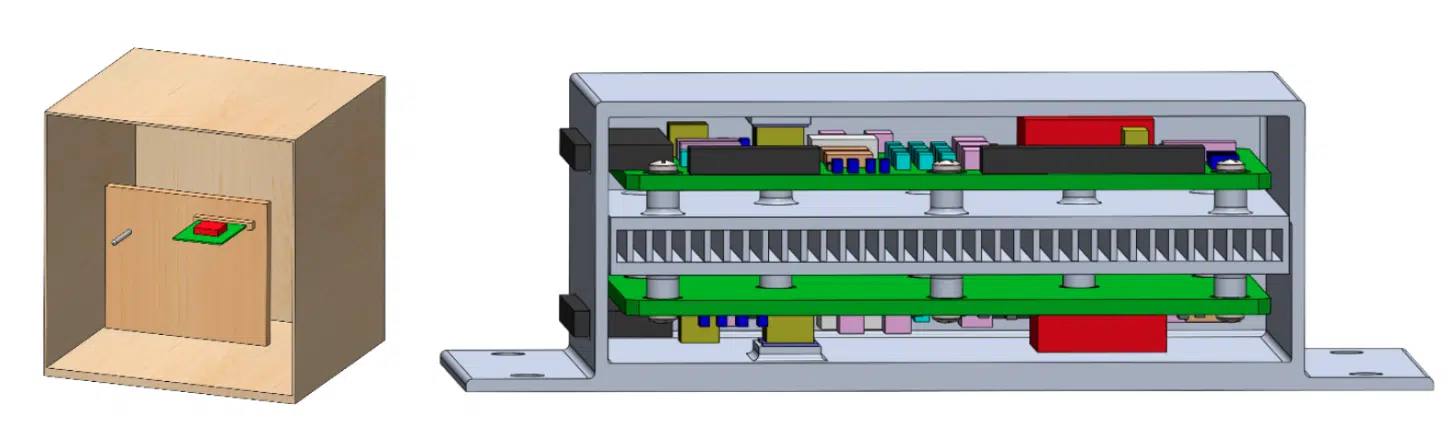
To illustrate the difference in primary heat transfer paths between the JESD51-2A standard and a sample electronics packaging application, consider Figure 1. The figure compares the test enclosure assembly specified in JESD51-2A and a typical circuit card application within a sealed enclosure. The circuit card contains an FBGA (red color) whose heat dissipation conducts into the circuit board, through standoffs, and finally into a heatsink cooled by forced convection.
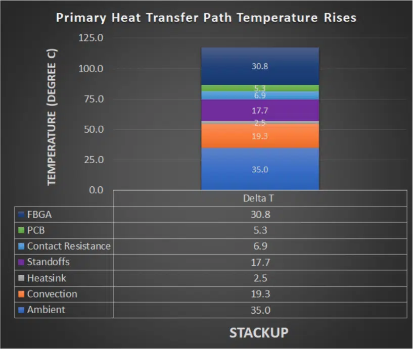
A stacked bar chart is an excellent method to demonstrate the multiple temperature rise contributions along the primary heat transfer path through the electronics assembly. These charts identify the largest contributors to temperature (i.e., “thermal bottlenecks”) based on the Pareto principle, which roughly states that many problems are due to few causes. In this case, θJB would be used to calculate the temperature rise from the board to the component junction and θJA would be disregarded for this analysis. A sample stacked bar temperature chart is presented in Figure 2.
Conclusion
The use of θJA to calculate junction temperatures of circuit card components is typically a misapplication of the θJA parameter. Doing so will often yield an incorrect estimate that can give the engineer a false sense of security in the mechanical and electrical designs of an electronics assembly. Instead, a detailed thermal analysis should be performed, and the θJA parameter should only be used during the initial circuit card design stage of component selection. The proper methodology for calculating junction temperatures is with a detailed conduction or CFD model of the electronics assembly – or alternatively, with components’ junction-to-board thermal resistances, θJB, if the substrate temperatures are known. With this manuscript, the authors aim to provide a central reference of the technical reasons why θJA should not be used to estimate an electronic component’s junction temperature.
References
[1] B. Joiner, “Use of junction-to-board thermal resistance in predictive engineering,” Electronics Cooling, 1999, https://www. electronics-cooling.com/1999/01/use-of-junction-to-board-thermal-resistance-in-predictive-engineering/
[2] B. Guenin, “Determining the junction temperature in a plastic semiconductor package, part 1,” Electronics Cooling, 1999, https:// www.electronics-cooling.com/1999/05/determining-the-junction-temperature-in-a-plastic-semiconductor-package-part-1/
[3] R. Bornoff, “So, you want to predict component temperatures do you? Part III,” Electronics Cooling, 2009, https://www.electronics-cooling.com/2009/11/so-you-want-to-predict-component-temperatures-do-you-part-iii/
[4] Electronics Cooling Editorial Board, “Update on JEDEC Thermal Standards,” Electronics Cooling, 2012, https://www.electronics-cooling.com/2012/09/update-on-jedec-thermal-standards/
[5] “Process management for avionics – Electronic components capability in operation – Part 1: Temperature uprating” (Edition 2.0, Annex B), International Electrotechnical Commission (IEC), Technical Report 62240-1, 2018
[6] “Integrated Circuits Thermal Test Method Environmental Conditions – Natural Convection (Still Air),” JESD51-2A, JEDEC Solid State Technology Association, 2008
[7] “Integrated Circuit Thermal Test Method Environmental Conditions – Forced Convection (Moving Air),” JESD51-6, JEDEC Solid State Technology Association, 1999
[8] D. Edwards and H. Nguyen, Semiconductor and IC Package Thermal Metrics (Revision D), Application Note SPRA953D, Texas Instruments, 2024
[9] Package Thermal Characteristics, Application Note AC220, Microsemi, 2012
[10] H. Pape, “Thermal characterization of active components,” Electronics Cooling, 1999, https://www.electronics-cooling. com/1999/05/thermal-characterization-of-active-components/